Double-sided PCB Assembly: A Complete Guide to the Assembly Process
Introduction
Double-sided PCB, double-sided layer or double layer PCB are one of the most popular type in nowadays electronics for complexity and compact of circuit. At the heart of good double-sided PCB assembly is solder paste – the adhesive material which bonds the electronic components to the copper pads on the PCB. This one-stop-shop video is a masterclass to both solder paste and the double-sided PCB assembly method. If you are an engineer, maker, or electronics manufacturer trying to get the most out of your surface-mount assembly (SMT), here is where you’ll find all the good stuff — from selection and printing solder paste, to advanced inspection techniques, and troubleshooting.
Key Takeaways
- Solder paste is the key material for the good quality SMT and double-sided PCB assembly.
- Understanding solder paste composition and types provides two-sided PCB build yield and reliability.
- Monitoring the double-sided PCB assembly processes in detail is essential when you want to have a stable manufacturing outcome.
- Advanced testing including Automated Optical Inspection (AOI) and In-Circuit Testing (ICT) reduces the fabrication defects dramatically.
- Cleaning, safety, and best practice recommendations for long life and good performance of double-sided PCB products.
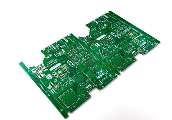
What Is a Double-Sided PCB?
A double-sided PCB (or two-sided/double-layer PCB) has circuit and copper traces on both sides of the board, that are joined with plated holes (vias). This is a key design for medium complexity circuits where one layer is not enough and multi-layer construction is not needed. Double-sided PCBs provide:
- Denser Component Placement – Components can reside on both sides, saving board space.
- Improved Circuit Routing – Connections can cross over between layers via vias.
- Cost-Effective Prototyping – Less expensive than multilayer boards for many moderate-complexity products.
History and Evolution of Solder Paste and Double-Sided PCBs
Soldering has been around for thousands of years, but the development of solder paste designed for the automated assembly process is fairly new. As electronics shrank in size, pressing consistency to attach tiny surface-mount devices (SMDs) drove the innovations that led to today’s solder pastes and the PCB assembly process.
Evolution Highlights
| Era | PCB Technology | Assembly Advancements |
| 1970s-1980s | Single-sided, hand solder | Solder wire, dip soldering |
| 1980s-1990s | Double-sided PCBs emerge | Solder paste, SMT, stencils |
| 2000s+ | Multi-layer, HDI designs | Dual reflow, automated AOI |
The double-side PCB was firstly widely applied into consumer products, which made the shift to smaller, denser, and more complex electronics possible. Nowdays, the double-sided PCB assembly is the basic for EMS (Electronic manufacturing services) provider.
The Role of Double-Sided PCBs and Solder Paste in Modern Electronics
Double-sided PCBs allow for small, dependable devices for all kinds of industries. The combination of a strong board design and the correct solder paste selection results in electrical, mechanical, and process of manufacture good results.
Typical Applications
- Consumer Electronics:Smartphones, wearables, gaming devices
- Automotive:Engine control units, in-car entertainment
- Medical:Portable patient monitors, diagnostic tools
- Industrial:Control panels, automation equipment
With the use of the right solder paste, it is possible to obtain good solder wetting and flux activation, a reduction in the number of soldering imperfections and assured component bonding by wave, reflow or manual assembly.
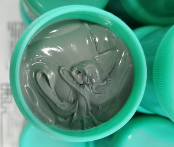
What Is Solder Paste?
Solder paste is a paste (actually a suspension of flux and solder powder) with the consistency of very viscous peanut butter. It is applied to the PCB pads (typically using stencil printing or dispenser method) as temporary “glue” to hold the SMD the component in place during the reflow soldering. During reflow soldering the solder paste melts, creating strong, conductive bonds between pads and leads.
Key Functions
- Ensures precise component positioning before soldering
- Activates oxide removal for reliable solder wetting
- Provides mechanical and electrical joint integrity after reflow
Composition of Solder Paste
Knowledge of solder paste composition is important for choosing the appropriate paste for two-sided PCB assembly.
| Component | Role |
| Alloy Powder (Sn-Pb, SAC, etc.) | Melts to form solder joint |
| Flux (rosin, no-clean, water-soluble) | Cleans pads and enables solder flow |
| Additives (surfactants, stabilizers) | Enhance printability, shelf life |
Common Solder Paste Types
| Variant | Alloy Composition | Melting Point | Best Use Case |
| Tin-Lead (Sn63/Pb37) | 63%Sn/37%Pb | 183°C | Legacy electronics |
| SAC305 (Lead-Free) | Sn/Ag/Cu | 217–221°C | RoHS-compliant modern electronics |
| Low-Temp (Sn/Bi/Ag) | Sn/Bi/Ag | 138–170°C | Thermally-sensitive assemblies |
Types of Solder Paste for Double-Sided PCB Assembly
In the assembly of double-sided PCBs, the type of solder paste and flux chemistry influence the yield and the reliability.
Selection Considerations
- Alloy Type:Leaded vs.lead-free, sensitivity to application temperature
- Flux Type:No-clean (with little after-cleaning), water-soluble (needs wash), RMA (rosin mildly activated)
- Particle Size:Finer powders for fine-pitch or micro-BGA devices (Type 3, 4, etc.)
- Specialty Needs:Solder pastes for sensitive or green applications – low temperature or halogen free.
Table: Solder Paste Types for PCB Assembly
| Solder Paste Type | Pros | Cons |
| No-Clean | Less cleaning, fast process | May leave benign residue |
| Water-Soluble | Cleanest joints | Needs wash, risk of corrosion |
| RMA | Middle ground | Not always RoHS-compliant |
Preparing for Double-Sided PCB Assembly
Preparation is essential to the success of any PCBA process, more so for double-sided PCBs.
Steps Before Assembly
- BOM & Assembly Drawings:Make the assembly the BOM and detailed assembly drawing depicting part location and orientation
- Workspace and ESD Setup:Establish an ESD-safe PCB assembly area with ESD mats and wrist straps to guard on sensitive parts.
- Component Organization:Label and pre-sort SMD/through-hole parts for easy access.
- PCB Surface Inspection:Check both surfaces for scratches, dust or Clean with a lint-free cloth and isopropyl alcohol (IPA) if required.
- Stencil and Solder Paste Prep:Choose the right amount of stencil thickness and solder paste for your board’s pitch and density.
Materials and Tools for Double-Sided PCB Assembly
To enable efficient processing of double-sided PCB assembly a range of materials and assembly tools are required, each suited to the complexity and density of your board’s design.The following checklist contains everything you need to be prepared for success.
Essential Materials
- Solder Paste:Choose based on component pitch, reflow temperature requirements, and drying requirements.
- Stencil:Stainless steel or nickel stencils for repeatable solder paste application. The thickness is usually 0.10~0.15 mm for normal SMT.
- PCB Panels:Ready-made double-sided PCBs, preferably with soldermask and clear silkscreen markings.
- SMT and Through-Hole Components:Check for all items to be complete and for any special treatment or positioning (such as Polarized Capacitors, IC notch marks, etc).
- Adhesives (for second-side reflow):Temporary bonding agents can be used for dense substrates or for bulky second-side parts.
Core Tools
- Pick-and-Place Machine:Precision pick and place of SMD components, with specific programs for double side mounting and component pooling.
- Manual Fine-Tip Tweezers:For precise positioning of the hand and compensation during the testing or repairing.
- Reflow Oven:Precise temperature profiles are possible during both first and second side soldering.
- Hot Air Rework Station:Use for reflowing single joints and repairs particularly in dense SMT layouts.
- AOI System:Automated Optical Inspection for after solder paste printing and component placement verification.
- Soldering Iron (Temperature-Controlled):For manual THT rework and touch-up.
- ESD Protection:Mats, wrist straps, ionizers—required in any professional PCB assembly environment.
- Cleaning Supplies:Isopropyl alcohol, soft brushes and lint free wipes for removing solder paste and flux.
Optional, But Valuable
- In-Circuit Test (ICT) System:For continuity, resistance, and operation checks of completed assembled boards.
- Conformal Coating Equipment:Essential for protecting PCBs operating in harsh environments.
Critical Double-Sided PCB Design Rules
Design for manufacturability (DFM) is the key to success in double-sided PCB assembly.Following are the key rules of thumb to for the engineers and PCB layout designers:
- Heavy Components First Place the largest/heaviest components on the primary (bottom) side if possible—these will be soldered first and are less likely to move in second-side reflow.
- Group by function and signal Place components of the same type, or closely related in terms of function, into logical groups this simplifies pick and place programming and the troubleshooting after assembly.
- Avoid stacking High-Density areas Stagger large groups of components across both sides to distribute the heat load and make placement easier.
- Polarity and Direction Marks Having a clear polarity, pin 1 and direction mark on the silkscreen is very important for an easy placement and visual check of the component.
- Consider Pick-and-Place Limitations Ensure your production line’s pick-and-place machine is capable of handling the smallest and largest parts, and design for that.
- Thermal Relief and Vias Apply thermal relief patterns to through-hole pads connected to large copper areas for good wave soldering or hand soldering.
Double-Sided PCB Assembly Process: Step-by-Step
1. Apply Solder Paste (Side A—usually underside)
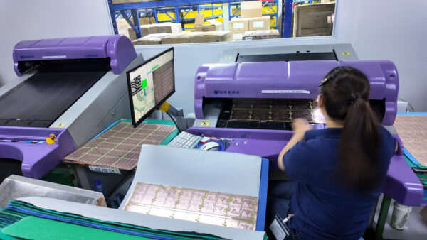
- Stencil Printing:Place the PCB and stencil on a printer, align and print solder paste. Spread uniformly using a stainless-steel squeegee. Look for uniform deposit-critical for fine-pitch devices.
- Dispenser Printing:For prototypes or repairs, manually dispense a few small controlled dots of solder paste where needed.
2. Place SMD Components (Side A)
- Use the pick-and-placemachine for fast and precise placement. The components are softly pressed into the adhesive solder paste while keeping orientation and polarity.
3. First Reflow Soldering (Side A)
Reflow Oven Profile:
- Preheat:Gradually ramp up to activate flux and avoid thermal shock.
- Soak:Allows even heat distribution.
- Reflow:The maximum temperature (245°C for SAC305, for example) melts the solder paste alloy.
- Cool Down:Slow, controlled cooling prevents thermal stress and joint cracking.
Check for tombstoning, bridging, or misalignment. Rework as needed.
4. Flip Board and Repeat for Side B
- Apply Solder Paste (Side B):If you are going to reflow-solder on two sides, print with stencil or dispenser on both sides.
- Place SMD Components (Side B):Lighter, smaller parts are ideal for this side.
- Dual Reflow:Apply optimized temperature profiles to avoid re-melting side A joints or shifting parts.
- Adhesives:For heavy or awkward parts apply dot of adhesive under part before reflow.
5. Insert and Solder Through-Hole Components
- After both sides are SMT-assembled and soldered, insert all through-hole parts.
- Soldering Options:
- Wave soldering for mass production
- Manual soldering is performed with a temperature-controlled fine tip iron for prototypes or small volume.
Solder Paste Application and Printing Techniques
Correct solder paste deposition determines yield and reliability.Monitor stencil parameters and printing methods carefully:
- Stencil Thickness:Thinner for fine-pitch (0.10mm), thicker for heavier pads (0.15–0.18mm).
- Squeegee Angle & Pressure:Standard angle is 60°, adjust pressure for full stencil wipe.
- Print Speed:Typical range is 25–50 mm/sec.
- Inspection:Utilize magnification or AOI to confirm the paste deposit; look for lack of paste, bridges, or blurs.
- Best Practice:Store solder paste in the refrigerator (2–8°C) and permit it to warm up to room temperature before use. Old paste will have poor printability and reliability.
Dual Reflow Soldering Challenges and Solutions
Advanced double-sided PCB assembly is susceptible to a number of unique defects.Understanding the root causes and mitigation is the key:
Component Displacement During Second Reflow: Gravity may pull heavier or unsupported items on the bottom to shift or drop. Apply the glue if needed, and treat the light elements for top side in dual reflow.
Thermal Profile Imbalance: Overheating can reflow previously soldered joints, causing shifts or weak connections. Utilize precision oven profiling tools and fine tune the ramp/peak time.
Solder Joint Reliability: Insufficient or too much amount of solder paste, poor quality of paste, and the wrong handling of these factors result in defective solder joint. Perform visual inspection and AOI after each reflow.
Flux Residue & Cleaning: Water-based pastes demand PCB washing with D.I. water or IPA after soldering. No-clean paste can leave small residues but see if you are planning conformal coating.
Post-Solder Inspection, AOI, and ICT
Inspection is non-negotiable in quality double-sided PCB assembly:
Automated Optical Inspection (AOI)
- AOI uses high-resolution cameras to scan assembled boards for:
- Solder paste volume and coverage
- SMD lead alignment
- Solder bridges, opens, and tombstoned parts
Visual Inspection
- Manual inspections for small base defects, particularly in small batches or prototypes.
- Inspect key areas: BGA spacing, polarity of components and solder joints difficult to inspect.
In-Circuit Testing (ICT)
- Electrical testing (continuity, resistance, shorts) to confirm real-world board
- Custom test fixtures may probe both sides simultaneously.
PCB Cleaning & Surface Finishing
Cleaning ensures dependability, especially for high-density and delicate circuits:
- Flux Residue Clearing:Rinse with IPA and scrub with a soft lint-free brush. For water-soluble flux, clean with warm deionized water.
- Conformal Coating:If needed, spray or dip coat the populated PCBs with protective materials after cleaning to offer protection from moisture, dust or chemicals.
Advanced Tips and Best Practices
- Optimize Your Reflow Profile:Adhere to the solder paste manufacture recommended temperature ramp rates and dwells. If applicable, profile each side individually.
- Thorough BOM and Assembly Drawings:Check the polarity, pin 1, and unique assembly instructions before manufacturing.
- Adhesive for Second-Side Reflow:Dot under heavy SMT components on side B before reheating.
- Segmented Assembly:Very dense or complex assemblies may also be produced in staggered runs, with QA/formal functional testing occurring between the stages.
Common Assembly Mistakes and Troubleshooting
| Defect Type | Root Cause | Remediation |
| Solder Bridging / Shorts | Excess paste, stencil misalignment | Adjust stencil, lower squeegee pressure |
| Tombstoning | Uneven paste, poor thermal profile | Rework profile, adjust pad geometry |
| Insufficient Solder (Opens) | Clogged stencil or expired paste | Clean stencil, use fresh paste |
| Shifted Components | Poor adhesive or reflow imbalance | Secure with adhesive, rebalance profile |
Frequently Asked Questions
What is a double-sided PCB?
A double-sided PCB (printed circuit board) is one of the most common types of PCB with components on both the top and bottom sides of the board and is known as two sided or double-layer PCB. Connections between sides are most often made through plated through-holes (vias).
What is solder paste and why is it important?
Solder paste consists of powdered solder alloy mixed with flux. It is printed on the pads of a PCB with a stencil or dispenser before the surface-mount components are placed. The paste melts and makes good mechanical and electrical connections when reflow soldered. For double-sided PCB assemblies, the proper selection of solder paste and application is critical to prevent common problems like bridging, tombstoning or insufficient wetting.
Can you do reflow soldering on both sides of a PCB?
Yes, dual reflow is standard for double-sided PCB assembly. Planning is necessary—heavier or heat-sensitive components should be mounted on the first side, and profiles should be customized to avoid re-melting previously soldered joints or moving components.
How are components placed on both sides of a PCB?
First, the solder paste is applied and SMT components on side A are placed, then reflow soldered. The board is turned over and the procedure is carried out on side B (usually for lighter components). Through-hole parts are generally hand-soldered or wave soldered after the SMT reflow. Pick-and-place machines, tweezers, and adhesives are necessary to achieve precision and reliability.
What are the major double-sided PCB assembly challenges?
Major challenges are maintaining component alignment in two-stage reflow, controlling thermal profiles, depositing adequate amount of solder paste, and avoiding common defects such as solder bridging and tombstoning. Sophisticated inspection (AOI), detailed documentation (BOMs, assembly drawings) and controlled environment (ESD protection) are required to meet the challenges.
How do you clean a double-sided PCB after soldering?
Cleaning is related to the flux type. Water soluble fluxes are generally rinsed with warm demineralized water. For no-clean pastes, IPA (isopropyl alcohol) and a lint free brush can be used to clean off residues. Conformal coating may be applied after cleaning to boards that will be used in severe environments.
Which solder paste is best for double-sided PCB assembly?
For most RoHS / lead free assemblies, a SAC305 based solder paste, tailored to your pad geometry and component pitch, is the best choice. Forletting the heat-sensitive boards, use low-temperature solder pastes. Always consult with the manufacturers recommendations and the paste shelf life.
Can you use expired solder paste?
It is not recommended. Degraded flux characteristics and oxidized solder particles may occur in expired solder paste products, which can result in the paste being difficult to print, having higher defect rates and producing unreliable solder joints.
Why is my solder paste sticky, dry, or runny?
Paste consistency problems are generally the result of stale or old material. Solder paste should always be stored refrigerated, brought to room temperature before use, and not be kept at room temperature or used for long periods.
Conclusion: Achieving Excellence in Double-Sided PCB Assembly
The secret to double-sided PCB assembly is an overall integration of comprehensive material usage, robust design rules and process structured sequential workflow execution. Solder paste is more than a consumable, it is a strategic enabler for high-yield, reliable electronics manufacturing.
Together with our ESD‒safe work place organization, stencil and reflow process optimization and 100% inspection by AOI and ICT you can be sure that your production will always result in boards which perform even in the toughest environments.
Before you work, check your BOM and assembly drawings, make sure the solder paste is suitable for the application and adapt the process to the complexity of the build. Take the time to understand the science and the art of solder paste and two-sided assembly and your PCBs will meet the reliability and performance goals demanded by today’s electronic products.
Lingkey provides process control and uniform production standards to high quality PCB fabrication and assembly process to assist, which contribute to the stability of yield and reliable performance of each assembly.


