Audio Amplifier PCB Design and Layout
Introduction to Audio Amplifier PCB Design
A superior audio power amplifier PCB is the backbone of all high fidelity sound systems, consumer and professional, in your home, the recording studio, or the manufacturer’s test line in the production plant. It’s more than just a simple interconnect, the performance of the amplifier board defines how cleanly it can amplify, how it handles noise, and how robust the long term operation is. For both professional and hobbyist users, knowing the essential factors of PCB for amplifier design—from layout basics to current flow patterns and advanced noise mitigation techniques—is critical. Just by learning the rules of PCB design, anybody can design a PCB which gives you clean powerful audio with tremendous noise rejection.
For custom audio amplifier PCB orders, the manufacturers like LingKey official website offer services of PCB manufacture and PCB assembly for prototypes and audio applications in volume.
What Is an Audio Amplifier PCB?
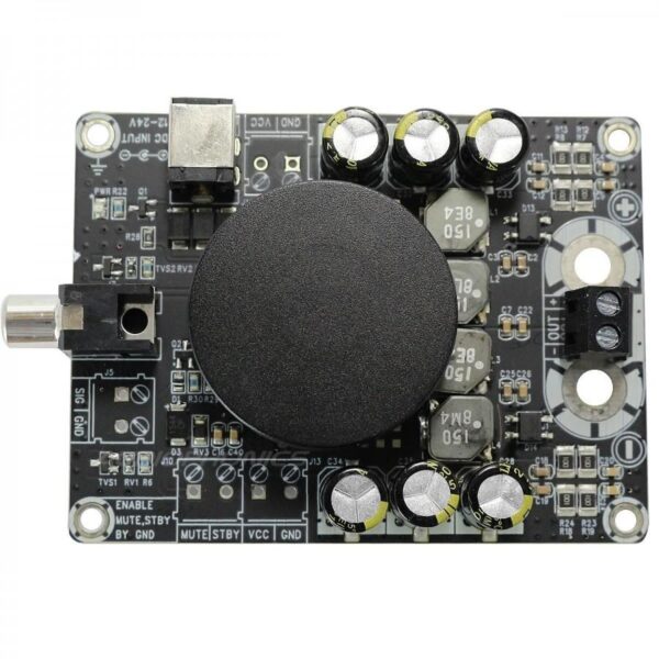
An Audio Amplifier PCB is a type of audio electronics PCB used to amplify and filter electric audio signals. The methodology for routing currents on these boards makes use of the carefully designed traces as the backbone which all other factors of an amplifier circuit’s components are connected. Good amplifier circuit board designs use methods that keep noise, heat dissipation and good solid ground lines to much as minimal as possible. This meticulous design process is what sets high quality PCBs apart from generic designs, isolating and preventing unwanted interference and ensuring a solid signal chain.
Amplifier Circuit Board Composition
- Layers: Most of modern amplifier PCBs are based on 2 or 4 layers, with the solid ground plane separated from the signal and power planes.
- Copper thickness: Audio & power amp builders often employ 2 oz (or thicker) copper for their power traces to support the higher current flow.
- Materials: FR4 is the norm for general audio hardware, whereas aluminium-core PCBs are reserved for situations where power dissipation is critical.
Tip: For custom PCB designs, provide additional mechanical support for heavy connectors or components subject to vibration—essential in mobile or automotive audio amplifier PCBs.
Types and Applications of Audio Amplifier PCBs
The most suitable amplifier designs are designed for particular uses of amplifier PCB—hi-fi, RF Amplifier, PA, or mini speakers. Every application has its own design considerations and considerations.
Types of Amplifiers
| Type | Key Features | Applications |
| Class A/AB | Linear; wide bandwidth; high heat output; premium sound quality | Hi-Fi amps, studio monitors |
| Class D | Digital switching; very high efficiency; requires low-pass output filtering | Compact speakers, portable devices, cars |
| RF Amplifier | Handles high frequencies; careful layout to avoid signal loss and electromagnetic interference | Wireless transmitters, radio gear |
Applications of Amplifier PCBs
- Professional audio systems (stage, theater, broadcast)
- Home and commercial wireless/Bluetooth audio
- High-power car amplifiers
- Instrument amplifiers
- RF communication equipment
Key Components of an Audio Amplifier PCB
A successful amplifier stage is composed of a variety of components, all meticulously selected and balanced, which provide certain attributes to noise in audio, linearity, distortion and reproducibility.
Active Components
- Op-Amps:Suitable for the preamps and tone control it is owing to their linearity and high input impedance.
- Transistors (BJTs, MOSFETs): Power stages are output in analog amplifiers; selected based on gain, bandwidth, and low ON resistance.
- Audio Amplifier ICs: The integrated nature of the solutions simplifies the design for novices and shortens the time to prototype for advanced amplifier designs.
Passive Components
- Resistors: Metal film types keep thermal and shot noise low.
- Capacitors: Ceramic or film for critical audio path, low-ESR electrolytic for power filtering and electrolytic decoupling caps.
- Inductors: Applied for output filtering; at best only usable in Class D or as RF stages to stop or let through certain frequency bands.
- Diodes: Protect from polarity reversal and voltage spikes.
Power and Decoupling Components
- Voltage regulators: Guarantee a stable supply, particularly critical for mobile and RF applications.
- Decoupling capacitors: Reduce ripple and local EMI, especially when connected inline to the IC power pins.
- Bulk capacitors: Provide energy reserve for high-current peaks in speaker outputs.
Connectors and Mechanical Hardware
- Use rugged, gold-plated connectors for reliability.
- Design with mounting holes and supports for heavy or vibration-prone setups.
Basic PCB Design Principles for Audio Amplifiers
- High-quality PCB design for audio is built on these principles:
Design Techniques & Guidelines
- Schematic clarity:Modularize and clearly label different amplifier circuit sections.
- Simulation:Validate your circuit before layout with SPICE or other simulation tools.
- Power/ground distinction:Use traces for power and ground with carefully calculated widths (see below).
- Solid ground plane:Never run ground wires in a daisy chain; utilize a solid ground plane for good low impedance and effective noise control.
Trace Sizing and Layout Rules
| Current | Recommended Trace Width @ 1oz Cu | Notes |
| 50-200mA | 10-15 mils | Preamp and line input/output |
| 1-2A | 40-50 mils | Typical power amplifier output |
| 5A+ | 100+ mils + multiple thermal vias | High power output, speaker connections |
- Layout rules: Isolate input from output; keep high-current nodes away from low-level signal traces.
- Via use: Hold vias for signal transitions between layers. For ground or power return, employ a via array (“stitching”) to reduce impedance.
Amplifier PCB Layout and Routing Best Practices
Advanced Layout Rules & Design Tips
- Component orientation:Maintain logic in orientation for easy assembly and debugging.
- Routing:Run input lines straight to preamps; keep power supply traces short and thick.
- Ground paths:Use star ground or dedicated ground return per stage; tie all to a central star point.
- Signal separation:The analog and digital grounds should be joined at only one point in order to prevent circulating currents.
- Guard traces:Place grounded traces between channels or on either side of high-impedance nodes to guard against crosstalk.
Noise Reduction and Signal Integrity
Professional Noise Reduction Methods
- Star grounding:Place all returns to one central low-impedance star; good for multi-channel or complicated amplifier PC boards.
- Continuous solid ground plane:Never break up the ground plane with signal or power traces, and always route signals over solid copper.
- Careful component placement:Input and feedback network elements should be located near op-amps input pins to reduce noise pickup.
- Shielded input section:Employ local copper pours or metal cans for the input stage, grounded to the main star point.
- Careful design of feedback and gain networks:Minimize trace lengths and add guard traces to keep external noise from coupling into high-impedance nodes.
Reducing EMI and Improving Signal Integrity
- Avoid loops by never letting input and output lines cross.
- Reduce noise by grounding all shields at a single point.
- For high-frequency or RF amplifiers, impedance-match traces and minimize stub lengths.
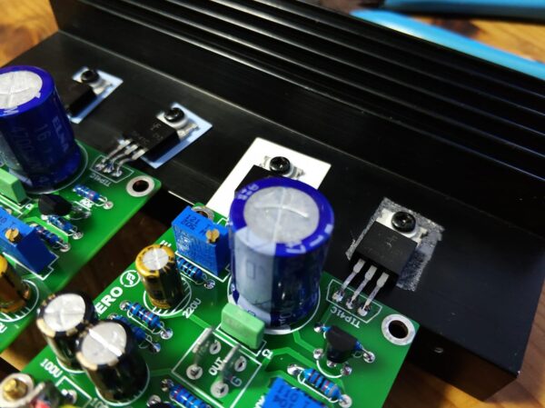
Thermal Management for Power Amplifier PCBs
Effective Design for Heat Dissipation
Since heat dissipation is one of the most vital features of a high-power amplifier PCB, it should be designed accordingly. With the greater current flow, there is an increased potential for heat buildup, which could affect the output of an amplifier, and even cause damage.
Design Tips for Thermal Management:
- Thermal Vias: Use thermal via arrays under power devices (such as output transistors, power ICs) to conduct heat from the component pads to the inner or bottom copper layers. The greater the number of vias, the lower the thermal resistance.
- Copper Pour for Heat Spreading: Widen power traces and fill large planes under hot components to improve heat dissipation. A good ground plane is also a heat sink for the board.
- Heatsinks and Heat Spreaders: Mount the heatsinks directly to the power devices or if possible, solder the devices to large copper areas. This is not unusual in tough amplifier designs or factory audio.
- Material Choice: For continuous-duty or high-power amplifiers choose aluminum-core (MCPCB) or thick copper PCBs. These materials have better thermal conductivity than regular FR4.
- Component Spacing: Leave ample space around high-power devices to avoid hot spots and to allow natural convection cooling.
- Forced Air Cooling: For the amplifier module designs used in racks or PA gear, lay out the PCB so that the major heat sources line up with the chassis fans.
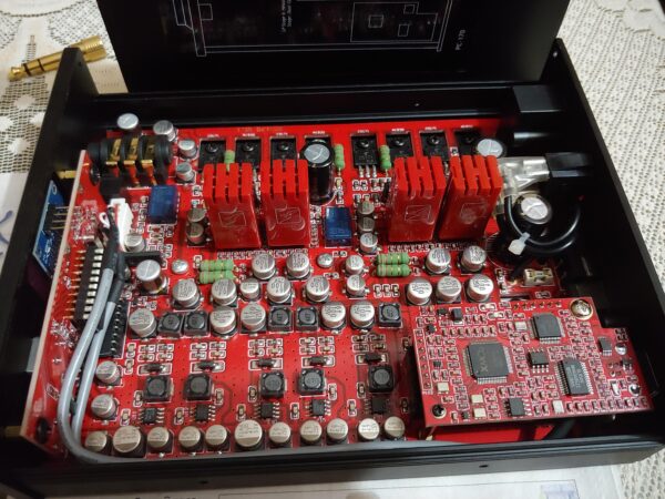
PCB Assembly & Manufacturing for Audio Amplifier Boards
An excellent audio power amplifier PCB is only as good as its build process. Every stage, including component placement and final testing, needs to be taken into account to ensure the finished amplifier provides the expected performance.
Assembly Practices for High-Quality PCB
- Surface-Mount Precision: Automated pick-and-place machine provides the best accuracy for SMD components which minimizes the assembly defects and enhances uniformity.
- Solder Paste and Stencil: Select the appropriate stencil thickness (4–5 mils) to achieve accurate printing of the solder paste. Proper paste deposition is essential for satisfactory solder joints on op-amps, audio ICs, and tiny passives.
- Reflow Profile: Use a controlled multi-zone oven. The reflow profile should ramp evenly and soak the PCB, then reflow and cool at a rate that avoids thermal shock and results in solder integrity.
- Automated Optical Inspection (AOI): Add AOI for every board to snatch placement errors, tombstones, bridges and bad solder joints—essentials for complicated amplifier layouts.
- Through-Hole (THT) Parts: For high load connectors, inductors, and power devices, THT assembly provides the necessary mechanical support for real-world applications.
Solder Joint Quality & Inspection
- Inspect solder joints using magnification or X-ray for fine-pitch ICs.
- For high current amplifier projects, visually inspect large power traces and joints for cold solder joints and ensure no voids of flux or solder have formed.
With LingKey official website as your experienced provider for PCB assembly, you can expect full service such as SMT assembly, AOI inspection, functional testing and turn-key manufacturing in your audio amplifier PCB project.
Testing, Validation, and Debugging
Performance Validation of an Amplifier Circuit Board
A good quality amplifier circuit should be verified by the functional test, not only a simple go/no-go test.
| Test | Objective | Instrument | Target |
| Output power | True RMS power under load | Dummy load, oscilloscope | As per design |
| Frequency response | Flatness, bandwidth, roll-off | Audio analyzer/sweeper | 20Hz–20kHz, ±1.5dB |
| Total harmonic distortion | Clean signal, no audible color | THD analyzer | <0.1% (hi-fi), <1% (basic) |
| Noise floor (SNR) | Measure of hum and hiss in output | Audio analyzer | >80dB SNR consumer, >100dB pro |
| EMI/EMC Compliance | Ensures board won’t emit or accept interference | Spectrum analyzer | As per regulatory class |
| Thermal soak | Reliability under elevated temp/load | IR camera, thermal couple | Days or hours at max load |
Debugging Tips
- If there is hiss or hum, check ground paths and decoupling capacitor placement.
- For distortion, probe feedback and signal paths for unwanted oscillation or excess gain.
- Extended load or soak testing is used to screen out failures caused by an underdesigned thermal solution or bad solder joints.
Component Placement Strategies
Strategic Component Placement
The right component placement is the key to reduce noise and have a good running of the amplifier. Practical design tips include:
- Position the inputs and preamp stages at maximum distance from the output and power supply sections, preferably at opposite ends of the board.
- Route feedback loops with the shortest possible leads to prevent outside pickup or phase shift.
- multi-channel power amplifier circuit boards mirror the left/right channels and use the same path for best case matching and stereo
Common Mistakes & How to Avoid Them
- Crossed power and signal paths:Ensure that high-current power traces are kept away from sensitive signal traces at all times.
- Improper ground return:Connect all returns at one star point, not haphazardly, and avoid ground loops like the plague.
- Insufficient thermal management:Undersizing power output stages results in failure problems.
- Failure to plan for assembly:Provide test points for critical voltages, include connector markings, and mechanically secure large or vibration-sensitive components.
- Neglecting EMI and RF interference:Particularly challenging for the audio and wireless (RF amplifier) signals on a dual amplifier board.
FAQs: Audio Amplifier PCB Design, Layout & Assembly
Q: What are essential design guidelines for noise in audio amplifiers?
A: Begin with a good ground plane, star ground your returns, separate power and signal, keep trace lengths to a minimum, and decouple every IC locally.
Q: Can I use the same layout rules for audio, power, and RF amplifiers?
A: No. RF amplifier PCBs require impedance matched traces, additional shielding and rigid isolation from the audio and power stages.
Q: How do you maximize performance of an amplifier with a custom PCB?
A: With simulation, test validation, thermal and electrical packaging optimization, and automated assembly with optical inspection for uniformity.
Q: How important is current flow in power amplifier boards?
A: Crucial. Small traces or bad layout constricts current and results in voltage drop, distortion and thermal problems. Power and ground traces should always be sized for worst case current.
Q: What’s the role of decoupling capacitors in high-quality PCB design?
A: Decoupling capacitors prevent power supply noise from being coupled into signal paths and should be used at every power pin of an active device.
Conclusion: Building a Reliable, Low-Noise Audio Amplifier PCB
A good audio amplifier PCB design isn’t influenced solely by the circuit design. Good PCB layout, ground plane, thermal management, signal routing and even assembly workmanship all influence noise floor, stable gain and long term reliability. From small size Class D modules to high power professional audio systems, at all levels of design and manufacture audio performance consistency is paramount.
Selecting a knowledgeable PCB fabrication partner that is experienced with the specific demands on audio electronics such as impedance control, heat dissipation, SMT assembly, and noise sensitive layouts is just as important. LingKey official site offers audio amplifier PCB fabrication and assembly service for your audio amplifier project, whether it is prototype, small volume production or mass production with dependable quality and engineering support.


